It all started with a team day presentation. The prompt was simple: give a 5-minute talk on any subject you want. For me, the choice was obvious. For years, I’d harbored a quiet ambition to build a Game Boy emulator from scratch - a rite of passage for many developers and a perfect blend of software engineering and retro nostalgia. So I thought I’d feed two birds with one scone and start doing some serious research.
The five minute talk flew by. The slides I presented1 were little more than prompts, skeletons of a much larger story I wanted to tell about the surprisingly elegant and complex heart of that little grey brick. This blog post is that story - a slightly expanded retelling of that original talk, born from the research that kickstarted my now-ongoing personal project: a fully functional Game Boy emulator written in Go.
So, grab a cuppa and join me on a journey into the architecture of one of the most beloved 8-bit handhelds ever made. You might be surprised by the engineering depth hiding just beneath the surface of this “simple” machine.
So, Which Game Boy Are We Talking About? Link to heading
Before we dive into the silicon, it’s crucial to define which “Game Boy” we’re dissecting. The Game Boy family isn’t a single device but a lineage spanning three distinct hardware platforms. First came the original 8-bit platform, which includes the iconic 1989 Dot Matrix Game (DMG). Next was the Game Boy Color, a significant but incremental upgrade that added color and a bit more power while maintaining backward compatibility. Finally, the Game Boy Advance arrived as a completely new ARM-based architecture, a powerful successor that could play older games but whose own games were entirely incompatible with the original hardware.
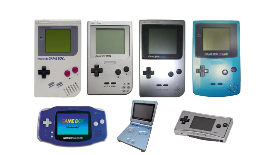
This post focuses on the original 8-bit architecture (top row of the above image). It’s the foundation for both the classic Game Boy and the Game Boy Color, and it’s the traditional starting point for any aspiring emulator developer.
It’s easy to forget just how revolutionary this device was. When it launched, it faced competition from full-color, backlit handhelds like the Atari Lynx and Sega Game Gear. But where those power-hungry machines chewed through batteries in maybe 3 to 5 hours, the Game Boy’s humble monochrome screen was a deliberate trade-off. That pragmatic choice for an efficient design delivered an incredible 15 to 30 hours of gameplay. This focus on longevity over flair won the market, cementing Nintendo’s dominance in the handheld space for decades. At the core of that efficiency was a unique and clever little chip.
The Heart of the Machine: The Sharp LR35902 CPU Link to heading
The Central Processing Unit (CPU) is the brain of any computer, and the Game Boy is no exception. Understanding its unique design is the first step in emulation. The chip at the heart of the Game Boy is the Sharp LR35902, a custom processor that tells a fascinating story of engineering heritage and pragmatic design choices.
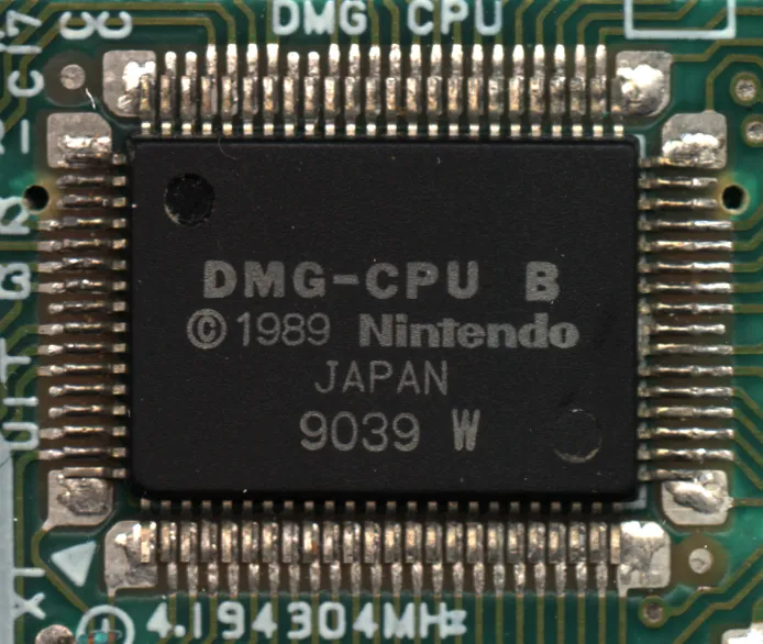
In fact, the LR35902 is a System on a Chip (SoC), meaning a single piece of silicon integrates the CPU core, graphics (PPU), sound controller, and I/O. This was a brilliant, cost-effective design that contrasted with consoles like the SNES, which used multiple dedicated chips.
Here are the core characteristics of this all-in-one powerhouse:
A Hybrid Heritage: Many documents, including my original presentation slides mischaracterise or over-simplify the chip as being essentially a stripped-down Zilog Z80 (of ZX Spectrum, Sega Master System & Pacman Arcade Cabinet fame). The reality is more interesting: the LR35902 is a custom hybrid. It inherits its core register set and instruction encoding from the venerable Intel 8080, but borrows a handful of powerful bit manipulation instructions from the Z80, leaving the rest of the Z80’s complexity behind.
The 4 MHz vs. 1 MHz Debate: The CPU’s clock crystal runs at 4.19 MHz. However, the system is fundamentally memory-bound; the CPU can only calculate as fast as it can access data from RAM. Since the memory bus runs at 1 MHz and most operations require memory access, the entire system is effectively paced at 1 million “machine cycles” per second. Thinking of it this way makes its performance much more comparable to other 1 MHz systems of the era, like the Nintendo Entertainment System.
Key Features: The CPU has a 16-bit address bus, allowing it to access up to 64KB of memory. Its design is incredibly power-efficient, a major contributor to the console’s legendary battery life. As a pragmatic choice for a simpler, more cost-effective chip, it lacks any dedicated hardware instructions for multiplication or division; these operations had to be performed in software.
Now that we have a high-level view of the CPU, let’s look at its internal workspace: the registers.
The CPU’s Short-Term Memory: Registers Link to heading
If the CPU is the brain, registers are its short-term memory. They are a small set of extremely fast storage locations built directly into the CPU chip. Instead of fetching data from the main system RAM every time, the CPU uses registers to hold the values it’s actively working on, making operations much faster.
For an 8-bit chip, the LR35902’s register set is beautifully simple and elegant:
General Purpose Registers Link to heading
The workhorses of the CPU are a set of 8-bit registers that can also be cleverly paired up to function as 16-bit registers, perfect for holding memory addresses.
| 15 … 8 | 7 … 0 |
|---|---|
| A (Accumulator) | F (Flags) |
| B | C |
| D | E |
| H | L |
The A register, or Accumulator, is special. It’s the primary register used for almost all arithmetic and logical operations.
Special Purpose Registers Link to heading
Two 16-bit registers handle the program’s flow.
| 15 … 0 |
|---|
| SP (Stack pointer) |
| PC (Program counter) |
- SP (Stack Pointer): Keeps track of a special area in memory called the stack, which is used for temporarily storing data, like the return address when a function is called.
- PC (Program Counter): This is one of the most important registers, as it always holds the memory address of the next instruction the CPU is supposed to execute.
The Flags Register Link to heading
The F register is unique. Its individual bits (or “flags”) are used to track the outcome of the most recent operation.
| 7 | 6 | 5 | 4 | 3 | 2 | 1 | 0 |
|---|---|---|---|---|---|---|---|
| Z | N | H | C | 0 | 0 | 0 | 0 |
Note that the lower four bits are unused and always read as zero.
- Z - Zero Flag: Think of this as a light that turns on whenever the result of a math operation is exactly zero. This is crucial for checking if two values are equal (by subtracting them).
- N - Subtract Flag: This flag simply notes whether the last operation was a subtraction.
- H - Half Carry Flag: This is a specialized flag used for handling complex internal math. While crucial for certain low-level operations, it’s less commonly used in day-to-day game logic.
- C - Carry Flag: This turns on if an operation results in a value too large to fit in the register, like adding 1 to 255 in an 8-bit register. It’s also used to signal a “borrow” in subtraction.
With data held in these registers, the CPU is ready to act. But what actions can it actually perform? That’s defined by its instruction set.
The CPU’s Vocabulary: Instructions and Interrupts Link to heading
An instruction set is the complete vocabulary of commands that a CPU understands. This vocabulary covers everything from fundamental arithmetic (ADD, SUBTRACT) and logic (AND, OR) to memory operations (LOAD, STORE) and commands that control the flow of a program (JUMP, CALL). For more detail on the full instruction set check out the opcodes table.2
Just as important as the instruction set is the concept of interrupts. An interrupt is a signal from hardware that tells the CPU to immediately pause what it’s doing and handle a more urgent task. Think of it like a doorbell ringing while you’re reading a book. You put a bookmark where you are (the CPU saves its state), answer the door (the CPU runs special “interrupt handler” code), and then return to your book right where you left off. This mechanism is critical for a game console, allowing it to respond to real-time events.
The Game Boy has five hardware sources that can trigger an interrupt:
- VBlank: Triggered when the screen has finished drawing a full frame. This provides a “vertical blanking” interval - a safe, quiet moment for the game to update graphics data without causing visual tearing.
- LCDC: Triggered by the LCD controller for various screen-related status updates, allowing for more advanced graphical effects.
- Timer: Triggered by a configurable internal clock. This is perfect for timing events in the game, independent of how fast the main code is running.
- Serial: This is the lifeline for multiplayer gaming, firing every time a piece of data arrives from a friend’s console via the Link Cable.
- Joypad: Triggered the moment a player presses a button. This allows the game to react instantly, rather than wasting precious cycles constantly asking the system, “Is a button pressed now? How about now?”
Understanding these instructions and interrupts gives us the building blocks. Let’s see how they fit together in a simple program.
Hello World? Link to heading
A traditional “Hello World” program that prints text to the screen is far too complex for a quick example, as it involves the entire graphics subsystem. However, we can look at a tiny, three-instruction program to see how registers, memory, and opcodes work in concert.
LD A, $41       ; Load ASCII 'A' into register A
LD (0xC000), A  ; Store it in memory
HALT
So what’s actually happening here? Link to heading
LD A, $41: This is a “Load” instruction. It tells the CPU to take the hexadecimal value $41 (which is the ASCII code for the character ‘A’) and place it into the 8-bit Accumulator register (A).LD (0xC000), A: This is another “Load” instruction, but this one involves memory. The parentheses mean “the memory address of”. So, this instruction tells the CPU to take the value that’s currently in the Accumulator (A) and store it at memory address 0xC000 (in the Game Boy’s 8 KB of internal work RAM - WRAM).HALT: This one is simple. It tells the CPU to stop fetching and executing any more instructions until an interrupt occurs.
And that’s it! In three simple steps, we’ve loaded a value into the CPU’s short-term memory and then written it out to the main system RAM. It’s from these fundamental building blocks that every game, from Tetris to Pokémon, is constructed. This seeming simplicity, however, hides a vast and fascinating complexity.
Conclusion: The Rabbit Hole of a “Simple” Machine Link to heading
Unsurprisingly that original 5-minute presentation and indeed this blog post have barely scratched the surface. As I dove deeper into my emulator project, moving past the well-documented basics, I discovered the true challenge - and the real fun. The official manuals3 tell you how the Game Boy is supposed to work, but the secret lies in how it actually works, quirks and all.
As reverse engineer Joonas Javanainen highlighted in his incredible Disobey 2018 talk4, there are around 20 different hardware revisions of the Game Boy CPU alone, each with subtle, undocumented behavioral differences. These aren’t just academic curiosities; they have real-world consequences. He points to the game Pinball Deluxe, which works perfectly on real hardware but crashes on most emulators. The reason? The game’s code relies on a very specific, undocumented timing behavior - an “edge case” - that only accurate, hardware-verified emulation can replicate. Discovering these quirks is a core part of the challenge for any emulator author.
The ultimate takeaway is that the Game Boy, often dismissed as a simple retro toy, is a masterclass in efficient and clever engineering. Its perceived limitations hide a depth that makes it a perpetually rewarding subject for developers and reverse engineers. My own journey with the Go emulator is far from over and I’m certain this will not be my last post on the subject. With each new detail uncovered - each timing nuance, each hardware oddity - the rabbit hole only gets deeper, and I plan to keep exploring it.